A First In Integrated Nanowire Sensor Circuitry

Scientists at the U.S. Department of Energy's Lawrence Berkeley National Laboratory and the University of California at Berkeley have created the world's first all-integrated sensor circuit based on nanowire arrays, combining light sensors and electronics made of different crystalline materials. Their method can be used to reproduce numerous such devices with high uniformity.
Nanostructures made with specific chemical, electronic, and other properties have a number of advantages over the same materials in bulk. For example, a nanowire is an ideal shape for a light detector; being virtually one-dimensional, practically "all surface," a nanowire is not only highly sensitive to light energy, but its electronic response is greatly enhanced as well.
To be practical, however, the photosensors must be integrated with electronics on the same chip. And the materials that make an ideal photosensor are necessarily different from those that make a good transistor.
"Our integration of arrays of nanowires that perform separate functions and are made of heterogeneous substances — and doing this in a way that can be reproduced on a large scale in a controlled way — is a first," says Ali Javey, who led the research team. Javey is a staff scientist in Berkeley Lab's Materials Sciences Division (MSD) and an assistant professor in the Electrical Engineering and Computer Sciences Department at UC Berkeley. He and his colleagues report their work in the August 1 edition of Proceedings of the National Academy of Sciences (PNAS).
Printed arrays
To grow a crystalline material on another crystalline material is difficult if the crystal lattices of the two materials are highly mismatched. Lattice matching is a particular challenge when more than one kind of material must be assembled on the same substrate. While many nanowire devices involving circuitry have been created over the years, these have required carefully selected substrates and specialized assembly — devices that are virtually one of a kind.
"Our main objective is a route toward integrated nanowire arrays that we can produce on any substrate — even paper! — and to reproduce them uniformly on a large scale," Javey says. "To do that, over the past two years our group has developed methods of printing nanowire arrays. After first growing the nanowires on a donor substrate, we transfer them to any desired substrate, including paper or plastic."
The Javey group has devised two printing methods, contact and roller. The roller method involves growing nanowires on the surface of a cylinder and rolling it across the application substrate, like painting with a paint roller.
Contact printing involves growing nanowires on a flat substrate, inverting it, and pressing it onto the desired substrate. Then the nanowires are detached by sliding the growth substrate away, leaving them attached to the application substrate. Due to the lack of strong surface chemical interactions between nanowires, the process is self-limited to the transfer of only one layer of nanowires. The printed nanowires are highly aligned in the direction of the sliding.

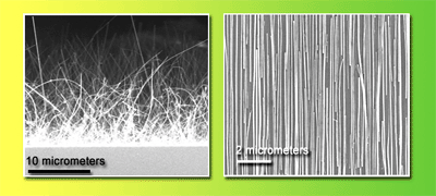
Randomly oriented nanowires, on the growth substrate at left, are having a "bad hair day." But after contact printing, the nanowires on the receiver substrate are highly aligned.
"This has an added advantage," Javey says. "Nanowires grow sticking out in random directions; they look like a bad hair day." But directionally sliding the array off the growth substrate, Javey says, "is like combing the hair to make it stand up straight."
This is a particular advantage because nanowire electronics need to be aligned for uniform performance. In the case of nanowire photosensors, alignment is essential for consistent response both to the intensity (brightness) of light and to its polarization, since the one-dimensional wires respond differently to polarization depending on their orientation. Because of their random orientations, the polarization response of "bad hair" nanowire arrays varies widely.
For their integrated nanowire photosensor circuitry, the Javey group used cadmium selenide nanowires as visible-light sensors. For the electronics, nanowires with a germanium core and a silicon shell were the basis of field-effect transistors that would amplify the current produced by the photosensors in response to light by five orders of magnitude.
Integrating the circuit
"To fabricate the integrated circuitry, we had to position the two kinds of materials at precise locations on the receiver substrate," Javey says. "The pattern for the device was on a photoresist layer coated on the substrate. First we printed the cadmium selenide nanowires onto the substrate, then removed the photoresist with acetone, leaving the cadmium selenide nanowires exactly where we wanted them. We repeated the process for the germanium/silicon nanowires."
The photosensors and the electronics were now positioned on the substrate as such elements might be mapped onto a much larger integrated circuit. (In the test case, a standard silicon/silicon-oxide substrate was used.) The circuit was completed by depositing metal electrodes to connect the elements; the resulting matrix of all-nanowire circuits, which acted as pixels, was used for imaging.
Results of the Javey group's integrated nanowire circuit showed successful photoresponse in 80 percent of the circuits, with fairly small variations among them. Where circuits did fail, the causes were due to defects in fabrication of the circuit connections (10 percent), failure in photosensor printing (5 percent), or defective nanowires (5 percent). The relatively high yield of complex operational circuits proved the potential of the technology, with improvements readily achievable by optimizing nanowire synthesis and fabrication of the devices.
"In the future, we can foresee using a variety of different optical sensors to create nanoscale devices sensitive to multiple colors in high-resolution," says Javey. "And that's just the beginning. We contemplate printing nanowire sensor circuitry — photosensors, chemical sensors, biosensors — not on silicon but on paper or plastic tape. This could be used, easily and with instant results, where spills have occurred, or to test air quality, or to test for disease organisms — almost any use for a sensor that you can imagine."
This research was supported by the Microsystems Technology Office of the Defense Advanced Research Projects Agency; Intel Corporation; and the Microelectronics Advanced Research Corporation — Materials, Structures, and Devices Center (MARCO MSD). Fabrication was performed at the Berkeley Microfabrication Laboratory. Nanowire synthesis was supported by a Laboratory Research and Development Grant from Berkeley Lab.
SOURCE: Lawrence Berkeley National Laboratory
